
Semiconductor Preconstruction Services for Fabs, Cleanrooms & Advanced Manufacturing Facilities
Optimar Precon provides Semiconductor Preconstruction Services for general contractors, EPC and design-build teams, fab owners, engineers, VDC teams and specialty contractors delivering semiconductor manufacturing and advanced technology facilities.
Our support includes semiconductor BIM services, cleanroom and sub-fab modeling, process utility and MEPFP coordination, structural BIM, CAD drafting, construction estimating, quantity takeoffs, shop drawings, Scan to BIM and technical documentation for defined project packages.
Optimar Group metrics
BIM & Preconstruction Support for Semiconductor Facilities
Optimar Precon supports defined semiconductor fab and advanced-manufacturing packages with BIM, cleanroom and sub-fab coordination, CAD drafting, estimating, quantity takeoffs and technical production support.
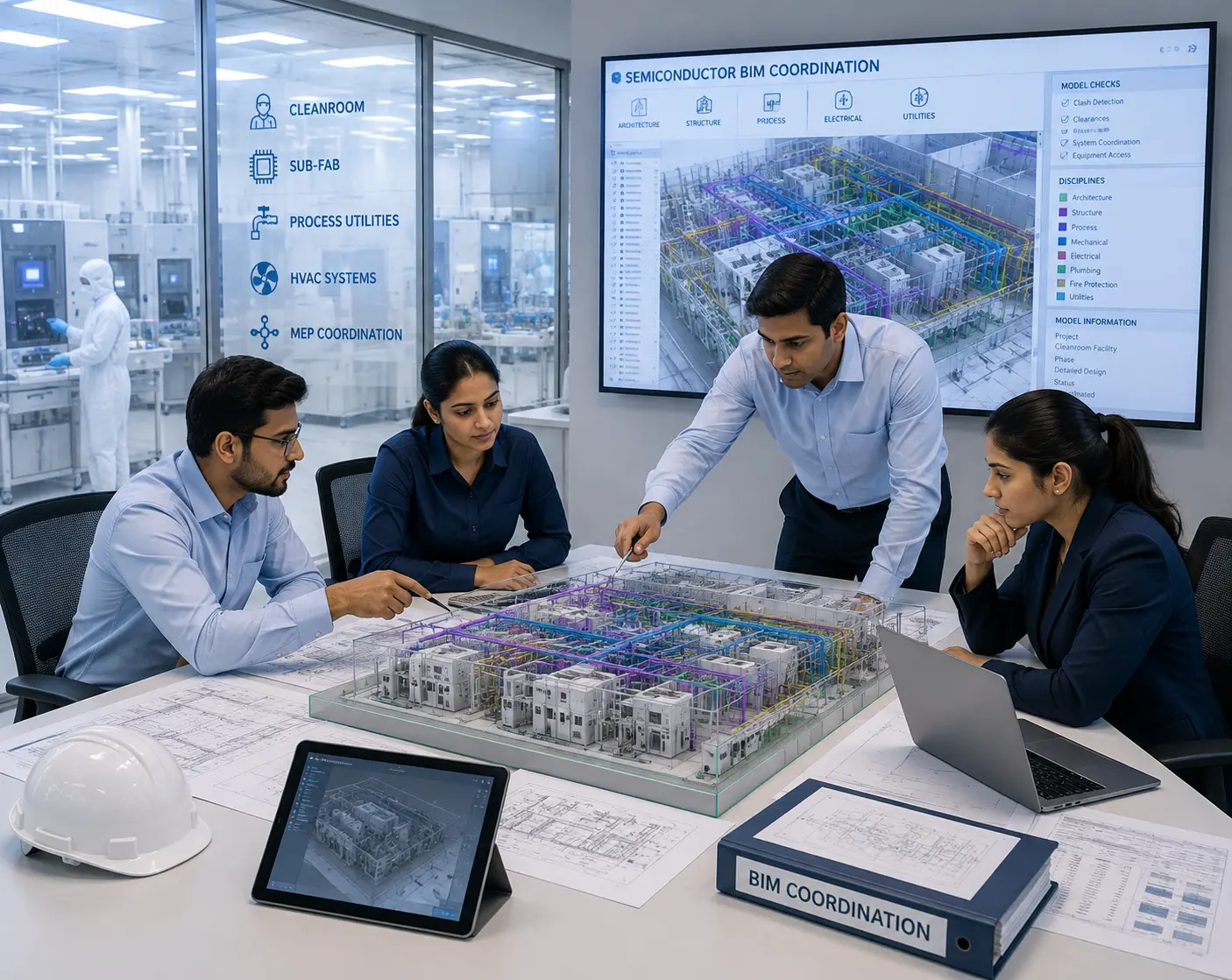
Coordinate Cleanroom, Sub-Fab & Building Systems Before Construction
Semiconductor facilities can contain dense overhead and below-floor services, technical equipment, structural systems and closely coordinated utility routes. Our teams develop and coordinate the assigned information from the current project sources.
Preconstruction Support for Defined Semiconductor Packages
Assign one technical production service or combine several disciplines around a defined fab, cleanroom or advanced-manufacturing package.
Semiconductor BIM Services
Develop coordinated BIM for defined fab, cleanroom and supporting facility packages.
Cleanroom BIM
Model and coordinate the assigned cleanroom architecture, structure and building services.
Sub-Fab BIM Coordination
Coordinate dense sub-fab systems, structure and utility routing information.
Process Utility Coordination
Coordinate supplied process-utility routes with structure and adjacent building systems.
CAD & Technical Drawings
Prepare technical drawings and documentation for clearly defined project packages.
Scan to BIM
Develop existing-condition BIM geometry from supplied point-cloud information.
Review Technical Interfaces Across Dense Semiconductor Facility Systems
Multidisciplinary BIM helps project teams review physical interfaces between cleanroom, sub-fab, utilities, structural systems and supporting building services within the assigned package.
Review supplied utility routes against structure, equipment and adjacent services.
Coordinate dense technical services within assigned sub-fab areas.
Bring supporting mechanical, electrical, plumbing and fire-protection information into coordinated models.
Review service routing and technical systems against structural framing and openings.
Review congested overhead zones where multiple systems share limited space.
Review documented interfaces between production levels and supporting technical spaces.
Support New Work Within Existing Semiconductor Facilities
For expansion and retrofit packages, our teams can use available drawings, BIM models, surveys and point-cloud information to support coordination between documented existing conditions and proposed project work.
Need support for a semiconductor project package?
Share the BIM, cleanroom, sub-fab, coordination, CAD or documentation scope.
A Structured Workflow for Semiconductor BIM & Preconstruction
Semiconductor packages can involve dense cleanroom and sub-fab systems, process utilities, structural interfaces and frequent project revisions. Our workflow keeps the assigned production package aligned with the current project information from review through delivery.
Review Inputs
Review drawings, BIM models, equipment layouts, utility information and project requirements.
Define the Package
Confirm the fab area, system, discipline and required deliverables.
Develop Information
Produce the assigned BIM, CAD, drawing or takeoff package.
Coordinate Interfaces
Review cleanroom, sub-fab, utilities, structure and services together.
Review & Deliver
Check revisions, coordination status and required final outputs.
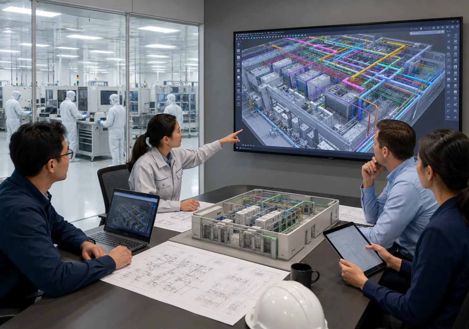
Keep Production Aligned With the Current Fab Package
Fab and cleanroom projects can move through equipment, layout, utility and discipline revisions. The assigned production package remains based on the current project information supplied by the project team.
- Current fab layouts
- Current discipline models
- Equipment layouts
- Process utility information
- Current project revisions
- Required deliverables
Common Coordination Checks Across Semiconductor Packages
Bringing cleanroom, sub-fab, process utility, structural and MEPFP information into one coordinated environment helps teams review physical interfaces within the assigned scope.
Review the Semiconductor Package Before Issue
The assigned package goes through production checks for scope, input alignment, model organization, coordination, revisions and required outputs.
Need support moving a semiconductor package through preconstruction?
Share the current drawings, models, equipment layouts, project scope and required deliverables.
Preconstruction Capacity for Semiconductor Project Teams
Add BIM, coordination, CAD, estimating and technical documentation resources to defined fab, cleanroom and advanced-manufacturing packages as project workloads change.
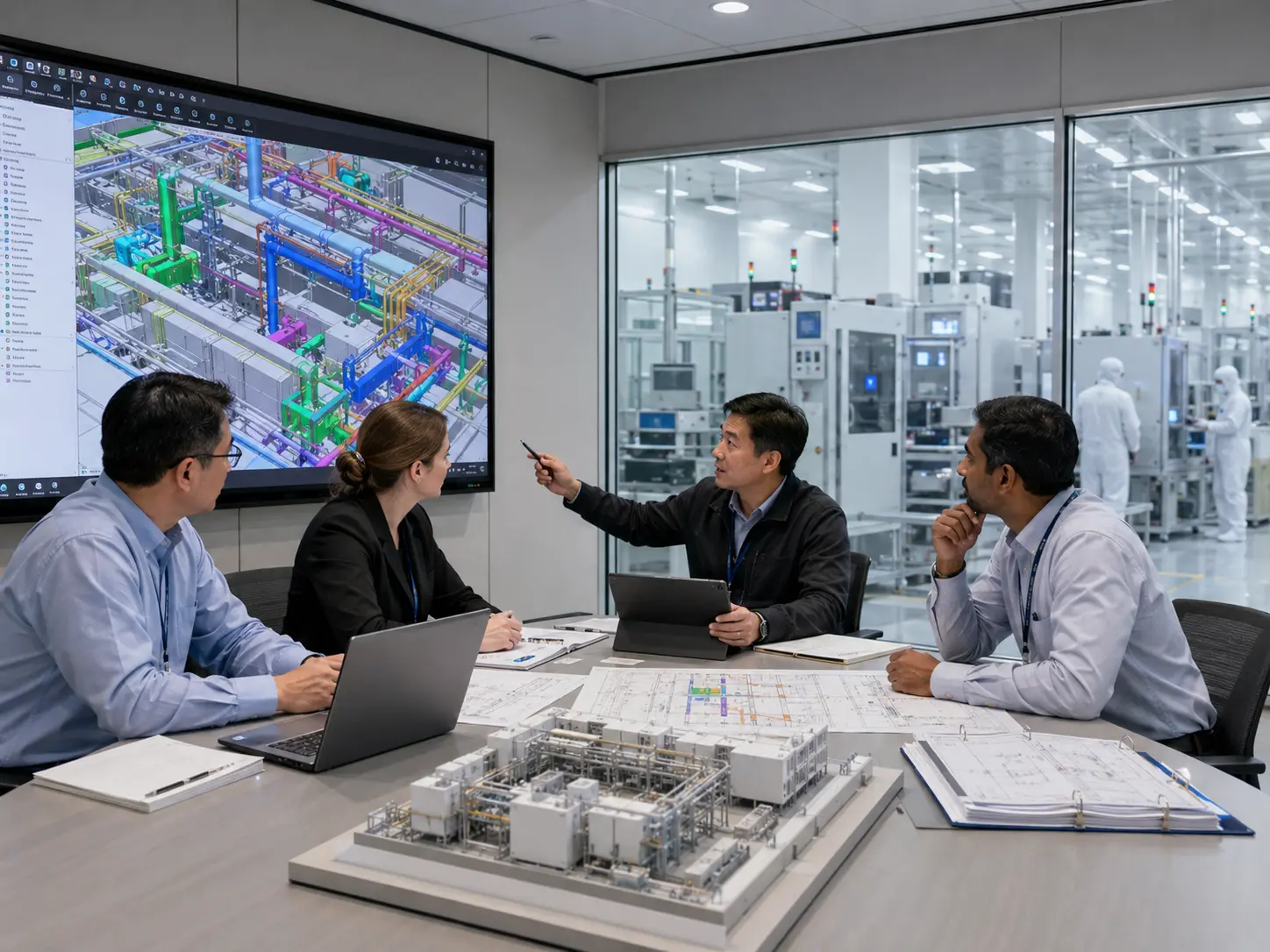
Technical Production Support Built Around the Assigned Fab Package
Semiconductor projects can create parallel workloads across BIM, cleanroom coordination, sub-fab systems, drawings, estimating and revisions. Our teams can support clearly defined production packages around the project information and outputs established by your team.
Package-Level Support
Assign one service, system, discipline or fab area.
Multidiscipline Capability
Connect cleanroom, sub-fab, structural, MEPFP and CAD production.
Revision Support
Add resources when layouts, utilities or project information change.
Scalable Capacity
Increase technical production resources around workload peaks.
Support Across Different Semiconductor Project Packages
Resources can be aligned with a fab area, project stage or technical package without assigning the complete semiconductor project.
New Fab Packages
Support BIM, drawings and coordination for defined new-build areas.
Fab Expansion Packages
Support additional cleanroom, utility and supporting-system scope.
Brownfield Retrofit Packages
Coordinate proposed work against documented existing conditions.
Coordination Packages
Review cleanroom, sub-fab, utilities, structure and MEPFP systems.
Tender & Bid Packages
Add estimating and quantity takeoff resources for defined scope.
Documentation Packages
Support CAD, shop drawings and technical documentation.
Production Resources for Semiconductor Project Delivery Teams
Our teams can work alongside contractors, EPC and design-build teams, engineers and digital-delivery professionals responsible for the assigned semiconductor package.
General Contractors
Add BIM, estimating and coordination production capacity.
EPC & Design-Build Teams
Support defined multidisciplinary preconstruction packages.
Specialty Contractors
Add modeling, coordination, takeoff and drawing resources.
VDC & BIM Teams
Add model-production and coordination resources during workload peaks.
Scale Resources Around Semiconductor Workloads
Add targeted resources when modeling, coordination, drawing, tendering or revision workloads increase.
Add model production for defined cleanroom, sub-fab or support areas.
Add resources during dense multidisciplinary coordination cycles.
Add CAD, shop drawing and documentation resources.
Add estimating and takeoff resources for defined packages.
Assign Only the Semiconductor Package You Need
Support can be structured around one service, one discipline, one fab area or additional production capacity.
BIM, CAD, estimating or documentation.
Structural, MEPFP, utilities or drafting.
One cleanroom, sub-fab area or technical package.
Ongoing production support across multiple packages.
Optimar Precon provides BIM, CAD, coordination, estimating and technical documentation production support from the project information supplied for the assigned scope. Semiconductor process engineering, tool engineering, process-utility design, equipment selection, cleanroom certification, engineering calculations, site verification and professional approvals remain with the responsible project team.
Need additional capacity for a semiconductor project?
Add BIM, CAD, coordination, estimating or documentation resources where the project needs them.
Questions About Semiconductor Preconstruction Services
Common questions about semiconductor BIM, cleanroom and sub-fab coordination, CAD, estimating and technical preconstruction support for fab and advanced-manufacturing projects.
What do Semiconductor Preconstruction Services include?
Do you provide BIM services for semiconductor fabs?
Can you support cleanroom and sub-fab coordination?
Can you support process utility BIM coordination?
Can you support existing fab expansion or retrofit projects?
Do you provide estimating and quantity takeoffs?
Can we outsource only one semiconductor package?
How is turnaround time determined?
Not sure what semiconductor project information to send?
Send the available drawings, BIM models, equipment layouts, utility information, specifications and project scope so the assigned production requirement can be reviewed.
Discuss Your Semiconductor Scope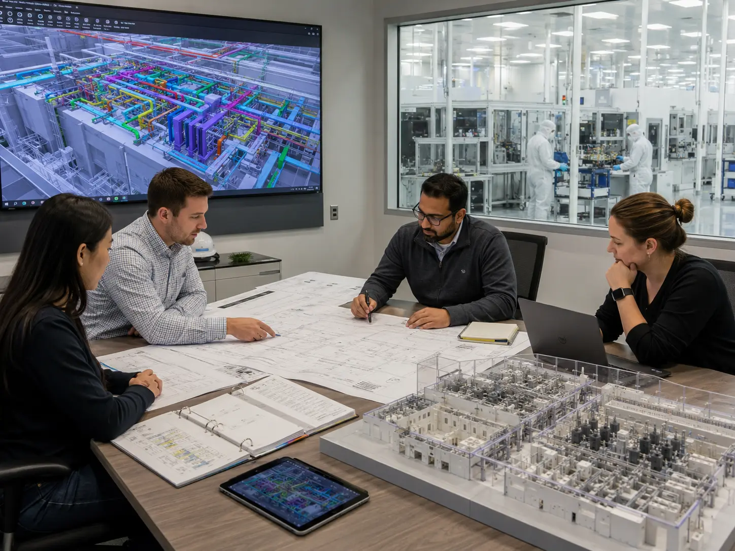
What to Send for a Semiconductor Preconstruction Package
The required information depends on the technical service and project stage, but the following items can help establish a clear production basis.
Typical Project Inputs
Potential Project Outputs
Four Details That Help Define the Semiconductor Package
A concise technical brief helps define the production scope, available project information and required outputs before the assignment begins.
BIM, CAD, coordination, estimating, takeoff or documentation.
Identify the cleanroom, sub-fab area, system or discipline.
List drawings, models, layouts, specifications and revisions.
Specify the models, drawings, quantities or documentation required.
Get a Quote for Your Semiconductor Preconstruction Package
Share your project scope, current drawings, BIM models, equipment or utility information and the technical outputs required.